Failure analysis (FA) is one of the tools that carries a lot of weight in the electrical and electronic (E&E) and manufacturing sectors as it determines what and how semiconductor products have failed.
The analysis is also to discover the best corrective action and to ensure continuous throughput improvement with lower operating costs. Thus, it is important for engineers, scientists and researchers to select the correct techniques, tools and interpretations of data to ensure a successful process of identifying and resolving a failure.
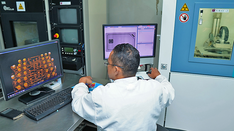
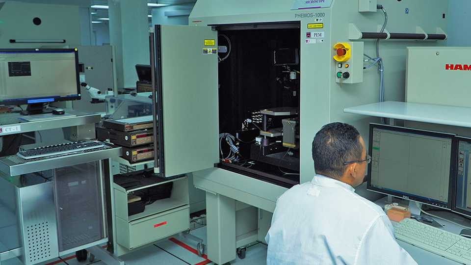
In supporting E&E’s long-term growth, MIMOS offers advanced analytical facilities including Failure Analysis and Material Analysis Lab which is equipped with world-class equipment and staffed by highly competent scientists and engineers.
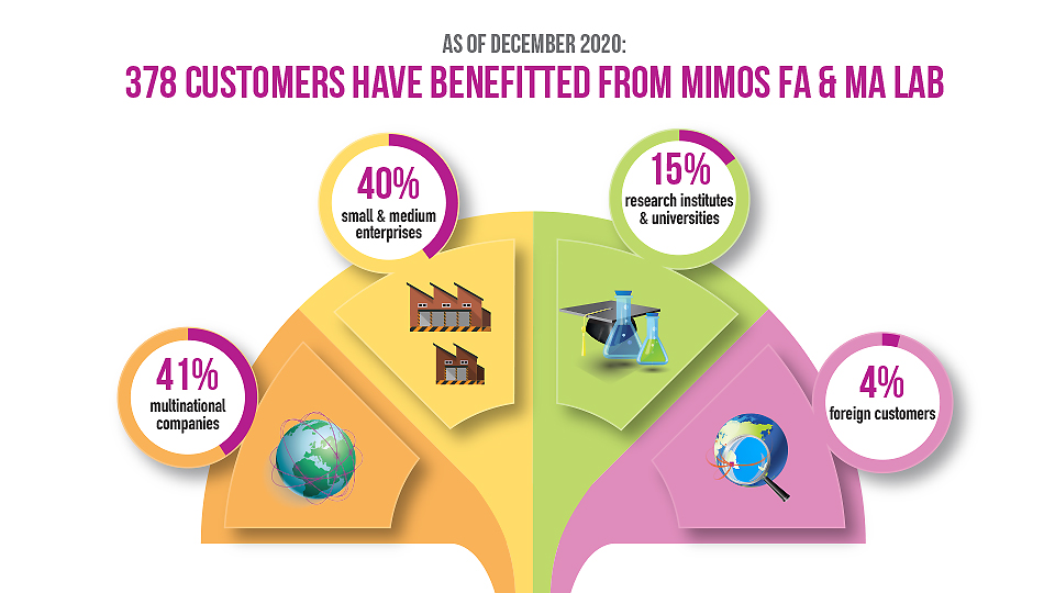
As of December 2020, the lab has benefitted 378 customers. Of the total, 41 percent were from multinational companies; 40 percent from small and medium entreprises; 15 percent from research institutes and universities; and 4 percent from foreign customers.
More than 1,300 types of services were rendered to the customers last year. MIMOS FA tools involve detecting failure mode, failure site, failure mechanism and root cause of failure.
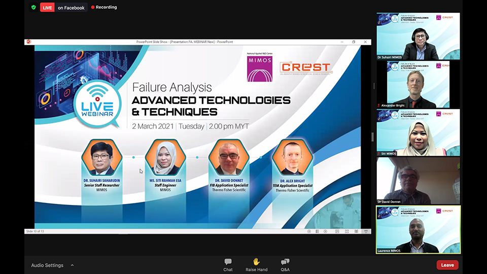
To highlight the latest analysis tools that can further improve the industry’s productivity performance, MIMOS held a webinar entitled ‘Failure Analysis Advanced Technologies and Techniques’ on 2 March.
The 2-hour webinar, held in collaboration with Collaborative Research in Engineering, Science and Technology (CREST), uncovered detailed methods and advanced tools available in the market.
Collaboration with CREST
The 2-hour webinar, held in collaboration with Collaborative Research in Engineering, Science and Technology (CREST), uncovered detailed methods and advanced tools available in the market.
MIMOS Senior Staff Researcher Dr Suhairi Saharudin said a successful failure analysis constitutes of process flow, conforming to the standard and quality practices, the right tools for required analysis as well as having skilled and experienced workforce, among others.
MIMOS Staff Engineer Siti Rahmah Esa later elaborated on several case studies comprising circuit modification for reverse engineering, embedded defect analysis, copper oxidation analysis and surface contamination analysis.
The session saw speakers sharing reviews on techniques, facilities offerings and some key technologies for semiconductor device imaging and analysis applications.
Add Content Here
Add Content Here
Add Content Here