Overview
A pristine graphene material on 8-inch (200mm) wafer for enabling the manufacturing and development of next generation high performance electronics.
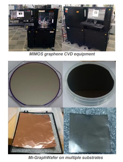
MIMOS Mi-GraphWafer is a state-of-the-art process technology for the development of pristine Graphene on 8-inch (200mm) wafer to enable the manufacturing and production of next generation advanced electronics. The graphene layer developed are available at the highest purity as well as uniformly-synthesised through industry-grade chemical vapour deposition (CVD) process technology.
Technology Summary
Mi-GraphWafer
State-of-the-art process technology for the development of pristine Graphene on 8-inch (200mm) wafer to enable the manufacturing and production of next generation advanced electronics.
Industries: E&E industries, SMEs, Government
Features
- High purity
- Uniform
- Large area
- Customisable
Technology Benefits
- Pristine graphene material
- Scalability
- Enabling new nanomaterials development
Mi-GraphWafer comprises the following features:
Features
Mi-GraphWafer comprises the following features:
- High Purity
Pristine single layer graphene synthesised through chemical vapour deposition (CVD) method on wafer. Can be tuned for biand multi-layer graphene. - Uniform
Single layer graphene coverage >90%. Top and bottom heater for uniformly-controlled growth and coverage. - Large Area
Can be synthesised on substrate of up to 8” (200mm). Also accept small sample size. - Customisable
Can be tuned and structured based on requirements and applications.
Technology Benefits
The main impacts of Mi-GraphWafer are:
- Pristine Graphene Material
High purity single layer graphene that can be transferred and utilised as a nanomaterial by itself for R&D and device development purposes. Quality of graphene controlled at a consistent and uniform manner across the substrate. - Scalability
Process capability-ready. Structuring and patterning of graphene material can be executed on full wafer-scale level for device development. - Enabling New Nanomaterials Development
Functionalisation of base graphene material can be achieved through multiple process add-ons for value-added purposes. Matured industry-grade chemical vapour deposition process
technology utilised.