


Technology Fact Sheets
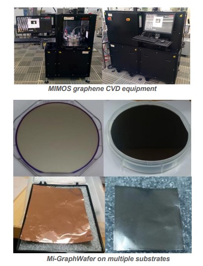
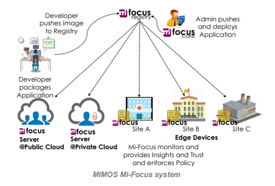
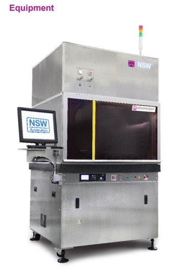
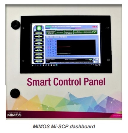
MIMOS has developed technologies and services for the enablement of technology growth. Download the following fact sheets for more details on our technology platforms.
MIMOS has developed technologies and services for the enablement of technology growth. Download the following fact sheets for more details on our technology platforms.
MIMOS Berhad
199501006785 (336183-H)
Taman Teknologi MRANTI,
Bukit Jalil, 57000 Kuala Lumpur,
Wilayah Persekutuan
Tel: +603-8995 5000
Fax: +603-8996 2755
E-mail: info@mimos.my
Our Location