
By Mohd Ibnu Haikal Ahmad Sohaimy (Senior Engineer), Failure Analysis Lab, MIMOS Berhad
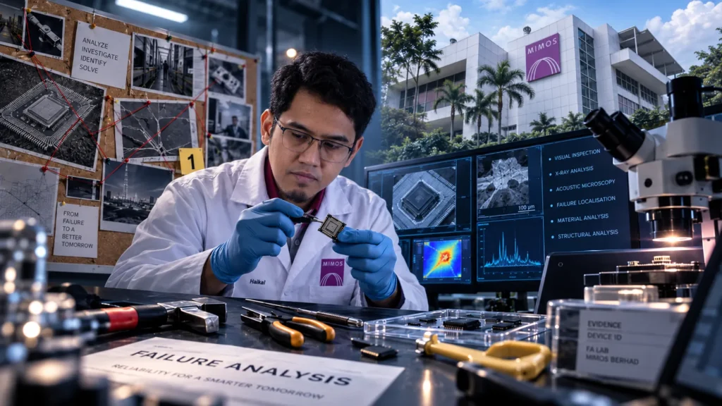
Most of us are familiar with Crime Scene Investigation (CSI) through news headlines, popular TV shows, movies, and video games. These depictions give us a captivating look into how investigators piece together evidence. But while traditional CSI focuses on human cases, engineering applies these same forensic principles to non-living systems. In this article, we take a look behind the scenes at how failure analysis engineers investigate complex problems inside semiconductor devices at the nanoscale.
Every Failure Has a Story (The Case Begins)
Every investigation begins with a sudden, unexplained event. Imagine scrolling through your phone late at night. Without warning, the screen flickers and dies while the sound continues playing in the background. To a consumer, this is a frustrating defect that leads directly to a warranty return. To an electronics manufacturer, failures like this, whether they happen in the hands of a customer or on the assembly line, signal significant risks, from costly recalls to lost reputation.
(Picture credit to – Siobhan Howerton, Pexel.com)
Semiconductor devices rarely fail without cause; rather, a subtle sequence of physical or electrical events leads to the ultimate breakdown. For a Failure Analysis (FA) engineer, a failed device is equivalent to a crime scene. Uncovering what went wrong at the nanoscale demands far more than sophisticated laboratory tools, it requires methodical logic and rigorous scientific inquiry.
Before an analyst picks up a single tool or opens the chip package, the investigation begins not with microscopic inspection, but with gathering the facts.
Know the ‘Victim’ Before the ‘Suspect’ (Understanding the Scene)
Every failure analysis begins with intake and context gathering. When a suspect device arrives at the lab, engineers first seek to understand its history by asking targeted questions:
- Failure Mode: What were the exact symptoms?
- Timeline & Context: When and where did the breakdown occur?
- Environmental Factors: Was the device subjected to electrical stress, heat, or moisture?
- Repeatability: Is the failure continuous or intermittent?
Much like criminal detectives interviewing witnesses to build a timeline before collecting physical evidence, FA engineers rely on this context to formulate testable hypotheses. Inadequate background data may lead to misguided analysis, wasted laboratory resources, and prolonged cycle times.
Every Clue Matters (Securing the Evidence)
Once the case history is established, the physical investigation begins. However, just like a crime scene investigator preserving fingerprints and footprints, a failure analysis engineer must follow a strict rule: do no harm to the evidence.
Before taking a chip apart, engineers must perform non-destructive testing (NDT) to inspect the device intact:
- External Visual Inspection: Examining the package under an optical microscope for mechanical cracks, discolouration, solder joint anomalies, or burn marks.
- X-Ray Radiography: Peering inside the moulded plastic to check for broken wire bonds, lead-frame shifts, or internal voids without opening the package.
- Acoustic Microscopy (C-SAM): Using ultrasonic waves to detect hidden internal delamination or sub-surface cracking between material interfaces.

(Picture credit to – cottonbro studio, Pexel.com)
Every surface anomaly, microscopic crack, or electrical anomaly is a critical clue. Gathering these early, non-destructive findings helps narrow down the location of the defect or area of interest and protects key evidence before moving to invasive testing.
With non-destructive clues gathered and candidate defect zones localised, the engineer moves from passive observation to high-precision diagnostic operations.
Choosing the Right Detective (Deploying the Specialists)
Once the initial examination is complete and candidate hypotheses are established, engineers call in the specialised instrumentation, the ‘big guns’ of failure analysis.
Just as criminal forensics relies on specialised experts (ballistics, toxicology, DNA profiling), microelectronics failure analysis requires specific diagnostic disciplines depending on the nature of the mystery:
- Electrical Failure Localisation: Tools like Photon/Thermal Emission Microscopy (PHEM / THEM) and Optical Beam Induced Resistance Change (OBIRCH) highlight exact locations of electrical leakages, shorts, or hot spots.
- Material & Chemical Analysis: Spectroscopy techniques such as Fourier-Transform Infrared (FTIR), Raman Spectroscopy, X-Ray Photoelectron Spectroscopy (XPS), and Time-of-Flight Secondary Ion Mass Spectrometry (ToF-SIMS) identify microscopic chemical contamination or unexpected material degradation.
- Physical Structural Analysis: High-resolution tools like Scanning Electron Microscopy (SEM), Energy-Dispersive X-Ray Spectroscopy (EDS), and Transmission Electron Microscopy (TEM) reveal nanoscale defects, physical cracks, or elemental distributions.
The engineer’s role is to exercise sound judgment in selecting the right tool for each specific question. A single piece of evidence is rarely enough; true confidence comes when independent findings from multiple tools converge on the same conclusion.

(Picture credit to – Maria Mileta, Pexel.com)
Like detectives reconstructing a crime scene, failure analysis engineers continually test their hypotheses against physical data. The goal is never to confirm an initial bias, it is to uncover the absolute truth at the nanoscale.
However, deploying state-of-the-art tools is only half the battle. The true challenge lies not in generating the data, but in interpreting what it actually means.
Evidence Doesn’t Speak by Itself (Reading the Clues)
Popular media often portrays forensic analysis as an effortless, instantaneous process: insert a sample into a black-box analyser, press a button, and immediately identify the culprit.
In semiconductor failure analysis, reality is far more nuanced.
Advanced laboratory tools, costing hundreds of thousands to millions of dollars, do not deliver ready-made answers. They deliver raw measurements:
- Spectrometers output peak intensities and chemical binding energies.
- Emission microscopes highlight localised heat or light emissions.
- Electron microscopes reveal physical topographies at the nanoscale.
An image showing a microscopic burn mark or a spectrum showing a carbon peak is just an isolated clue. The true core of failure analysis lies in data synthesis, connecting these individual clues back to physics, chemistry, and manufacturing context.
An experienced failure analysis engineer must answer critical diagnostic questions:
- Is this physical anomaly the primary cause of failure, or merely secondary damage caused by a prior event?
- Does this chemical trace originate from raw material contamination, or was it introduced during sample preparation?
- Does the electrical failure signature match the physical defect location?

(Picture credit to – Tima Miroshnichenko, Pexel.com)
The important point is that instruments produce observations, but experienced engineers determine what they mean. Without context and rigorous analytical reasoning, data is just noise. The true value of failure analysis lies in the engineer’s ability to turn raw evidence into actionable engineering insights.
Closing the Case (From Root Cause to Prevention)
In traditional crime scene investigations, identifying the perpetrator is the final goal: it brings closure and justice. In semiconductor failure analysis, however, discovering the root cause is only half the journey. The real objective is prevention.
Once the evidence converges and the root cause is pinpointed, whether it was a microscopic particle contamination, thermal stress, or a subtle design flaw, the failure analysis engineer presents the findings to process, package, and reliability teams.
Closing the case means transforming nanoscale forensic findings into concrete action:
Corrective Actions: Modifying manufacturing parameters to eliminate defects at the source.
Design Improvements: Refining component rules to withstand real-world electrical and thermal stress.
Quality Enhancement: Strengthening screening protocols to ensure defective units never reach the customer.
Ultimately, failure analysis is not just about dissecting what went wrong; it is about building stronger, more reliable technology for tomorrow. Every closed case strengthens the integrity of the next chip that powers our modern world.