By Ts. Dr. Siti Rahmah Esa, Head of Failure Analysis Lab, MIMOS Berhad
Have you ever dropped your smartphone, only to find that it still looked perfectly fine? Then, a few days later, the screen suddenly stopped responding, or the battery started draining unusually fast. Although there was no visible damage, something inside had already been compromised. This is a simple example of how appearances can be deceiving. The same situation occurs every day in industries such as semiconductor manufacturing, electronics, aerospace, and advanced materials. A product may pass quality inspection and look flawless on the outside, yet tiny defects hidden deep within the material can eventually lead to failure. The challenge is that these defects are incredibly small, often measured in nanometres, which are thousands of times smaller than the width of a human hair. Detecting them requires much more than a conventional microscope. It requires state-of-the-art electron microscopy, capable of revealing structures from the surface right down to the atomic level.
Every Failure Has a Story
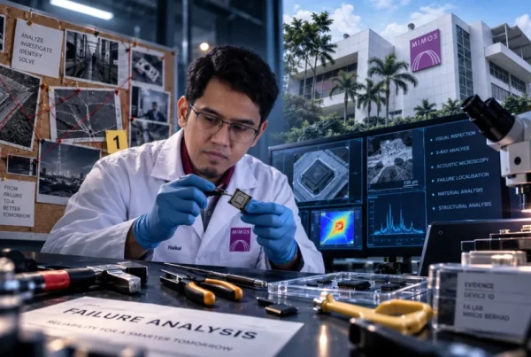
When a semiconductor chip stops functioning or a material cracks unexpectedly, the first question engineers ask is, “Why did it fail?” Finding the answer is much like solving a mystery. Imagine a detective investigating a crime scene. They do not jump straight to conclusions. Instead, they collect clues, examine evidence, and reconstruct what happened step by step. Failure analysis follows the same principle. Scientists search for microscopic clues that explain why a product failed. These clues may appear as tiny cracks, contamination, particles, voids, missing layers, or even slight changes in the arrangement of atoms. The ability to see these hidden details allows engineers not only to understand what went wrong but also to prevent the same problem from happening again.
Looking Beyond the Surface
A thorough investigation usually begins at the surface. Think of it like inspecting a second-hand car. Before opening the bonnet, you would check the paintwork for scratches, dents, or rust. These visible clues often tell you where to look deeper. Field Emission Scanning Electron Microscopy (FESEM) follows the same logic, but on a microscopic level. Using a finely focused beam of electrons rather than light, FESEM captures extremely high-resolution images to reveal tiny surface cracks, wear, contamination, and coating defects just a few nanometres wide. For semiconductor manufacturers, these surface observations are often the first step towards in pinpointing a root cause.
When Materials Need Gentle Handling
Not every sample can be examined under the same conditions. Imagine trying to photograph an ice sculpture under the hot afternoon sun. Before you capture the perfect image, the sculpture has already melted. Some materials behave similarly during microscopic analysis. Polymers, composites, ceramics, and moisture-sensitive materials can be easily affected under conventional high-vacuum conditions. This is where the Variable Pressure Field Emission Scanning Electron Microscopy (VPFESEM) becomes particularly valuable. VPFESEM allows delicate or non-conductive samples to be examined under gentler conditions while preserving their original state. Instead of changing the sample to observe it, scientists can study it much closer to how it naturally exists. This results in more reliable observations and ultimately more accurate conclusions.
Looking Beneath the Surface with Focused Ion Beam (FIB)
Sometimes, however, the surface only tells part of the story. Imagine slicing a layered cake. From the outside, every cake may look identical. But once you cut into it, you can see the different layers, fillings, air pockets, or imperfections hidden inside. FIB works in much the same way. By analysing a cross-section of a material, FIB reveals its internal structure, which cannot be observed from the surface alone. It enables researchers to examine grain boundaries, interfaces, particles, and defects buried beneath the surface. In modern semiconductors, where ultra-thin layers are stacked with extreme precision, this level of analysis is essential. Even a microscopic defect at a layer interface can degrade electrical performance and shorten the device’s lifespan.
Zooming in to the Atomic Level
Now imagine opening a map application. At first, you see an entire country. Then you zoom into a city, followed by individual streets, and finally a single building. Advanced microscopy follows a similar journey. FESEM gives us the bigger picture of the surface. But sometimes, even that is not enough. Using a high-resolution 300 kV Transmission Electron Microscope, scientists can observe materials at the atomic level. Atoms are the basic building blocks of every material. If just a few atoms are missing, misplaced, or arranged differently, the material may behave differently than expected. For advanced semiconductor devices, battery materials, and nanotechnology applications, understanding these atomic arrangements is becoming increasingly important. The ability to directly observe atoms allows researchers to understand why materials behave the way they do and how manufacturing processes can be improved.
Why Multiple Microscopes Matter
People often ask why one microscope is not enough. The answer is simple. When you visit a hospital, a doctor may first perform a physical examination. If needed, they might order an X-ray, followed by a Computed Tomography (CT) scan or Magnetic Resonance Imaging (MRI). Each test provides different information, and together they help build a complete diagnosis. Electron microscopy works in the same way. Each technique has its own strength.
· FESEM reveals surface details with exceptional clarity.
· VPFESEM examines delicate or non-conductive materials without damaging them.
· TEM provides atomic-scale information that explains material behaviour at its most fundamental level.
When these techniques are used together, scientists gain a complete understanding of a material from the surface all the way down to its atomic structure.
Why It Matters to All of Us
Although most of us will never see the inside of a semiconductor chip, we depend on these technologies every day. Our smartphones, laptops, electric vehicles, medical devices, renewable energy systems, and even household appliances rely on materials that must perform reliably for years. Every improvement in product quality begins with understanding why something failed. By identifying the root cause of failures, manufacturers can reduce defects, improve production yields, extend product lifespan, and develop safer, more reliable technologies. Ultimately, advanced microscopy is not just about producing remarkable images. It is about turning invisible information into practical solutions that improve the products we use every day. As technology continues to advance, our ability to see smaller details will become even more important. The next breakthrough in electronics or advanced materials may not come from building something bigger, it may come from understanding something smaller. Sometimes, the biggest engineering challenges are solved by looking at the tiniest details.
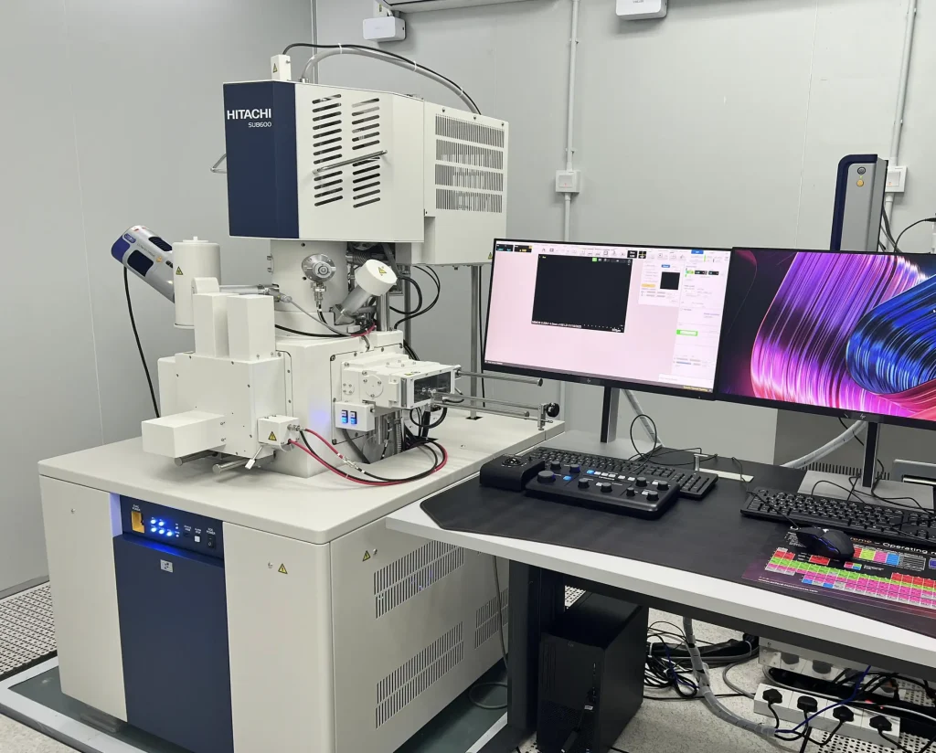
Field Emission Scanning Electron Microscopy (FESEM)
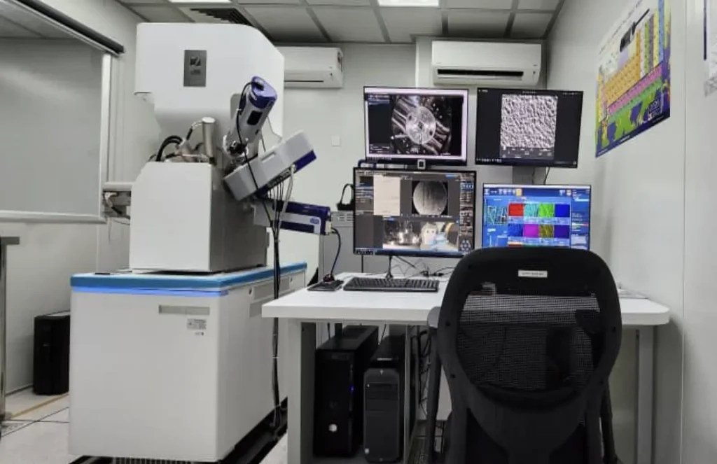
Variable Pressure Field Emission Scanning Electron Microscopy (VPFESEM)
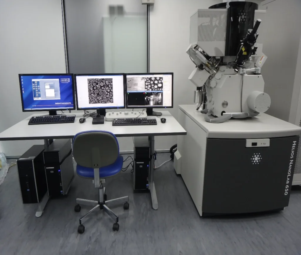
Focused Ion Beam (FIB)
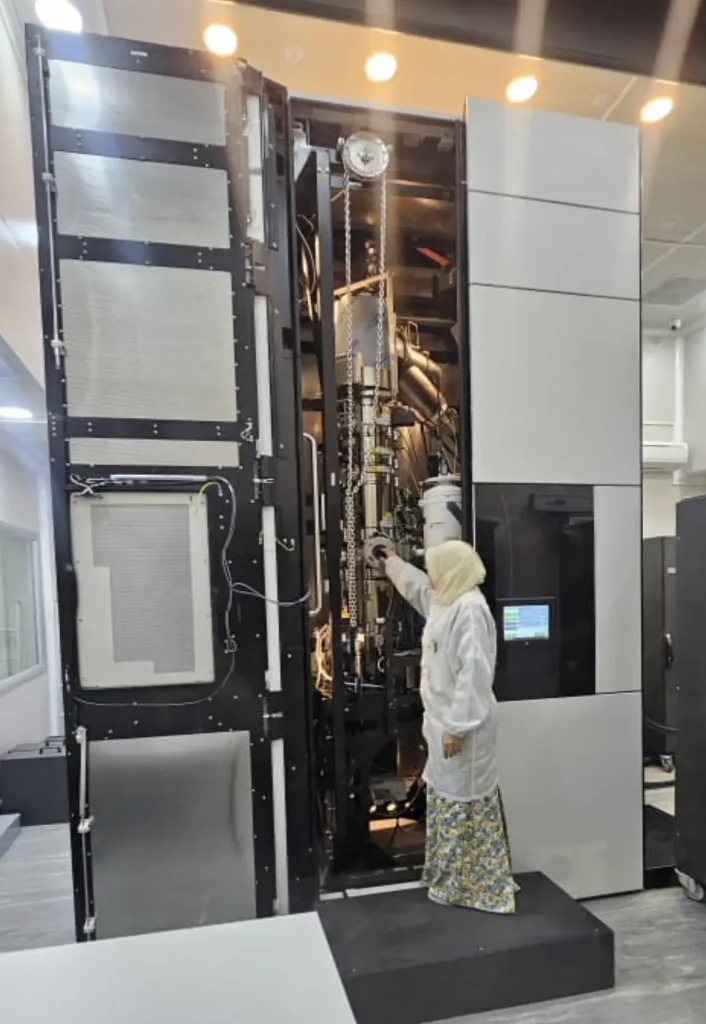
300 kV Transmission Electron Microscope (TEM)
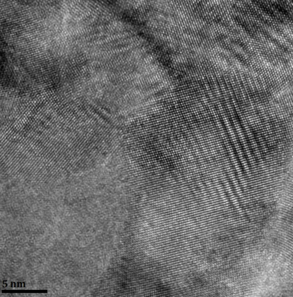
Atomic structure